Ultrasound is Our Strength
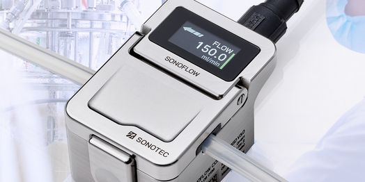
SONOTEC is a leading specialist in ultrasonic measurement technology solution based in Halle (Saale), Germany. With around 200 employees, SONOTEC develops and manufactures customer-specific ultrasonic transducers, sensors, testing equipment, and measurement technology solutions for Non-Invasive Fluid Monitoring, Preventive Maintenance, and Non-Destructive Testing.

Growth through Innovation with Ultrasound
SONOTEC was founded in the beginning of 1991 by the physicists Dr. Santer zur Horst-Meyer and Hans-Joachim Münch and has been family-owned ever since. In April 2019, Manuela and Michael Münch strengthened the management team of the business, while Dr. Santer zur Horst-Meyer moved to an advising role. With around 200 employees today, we are a growing technology company established on the market as a provider of products and solutions using ultrasonic measurement technologies.
We are Certified
TÜV Rheinland certified
Management System EN ISO 13485: 2016

TÜV Rheinland certified
Management System ISO 9001:2015

Do you have any questions?
Feel free to contact us! We will be happy to help you.

SONOTEC GmbH
Thüringer Str. 33
06112 Halle (Saale)
Germany


